
Research directions
The Department of Optics works at the crossing of six themes. One question unites them: what happens to light when it interacts with matter – and what that can tell us about the matter itself.
Below is not a list of the “department’s interests” but what people are working on right now. Behind each direction stand specific people, specific equipment and papers from recent years. If you are a student looking for a term project or a thesis, this is the page to read.
Advanced materials for optics and semiconductor optoelectronics
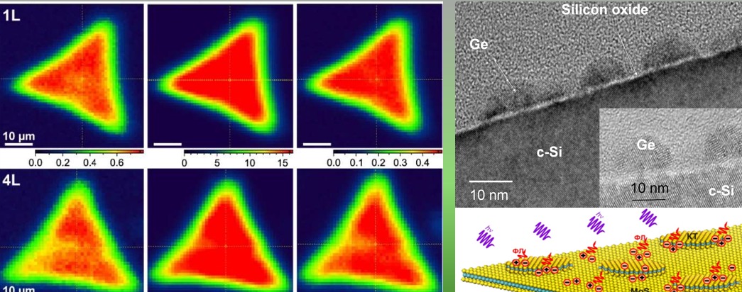
One of the strongest and most active research directions of the department. Developing and studying GeSn, InGaAs, CIGS, CZTS and other semiconductor materials for radiation sources and detectors, solar cells and optoelectronic devices.
The department studies how light-born charge moves in such films: where photoconductivity comes from, how defects and compositional inhomogeneity affect it, what happens at grain boundaries. Alongside GeSn – two-dimensional materials such as MoS₂ and quantum dot heterostructures: how energy and charge pass between layers one atom thick.
Among the methods: photoconductivity spectra from 10 K, impedance spectroscopy, scanning probe microscopy, photoluminescence, Raman scattering, electron microscopy.
Led by Serhii Kondratenko and Kateryna Yablochkova. Jointly with the Lashkaryov Institute of Semiconductor Physics of the NAS of Ukraine, the University of Arkansas and Chemnitz University of Technology. This is the line that produced the papers in Nanoscale and Physical Review Materials.
Solar energy
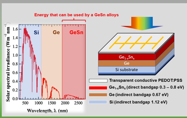
Developing and studying new materials and photovoltaic structures for the efficient conversion of sunlight into electricity and for next-generation solar cells; the direction is supported by international grants, including NATO, DAAD, DFG and CRDF Global. Silicon and germanium do not absorb the long-wave part of the solar spectrum – that energy is simply lost. GeSn, with its direct band gap of 0.3–0.8 eV, absorbs exactly that part, so a GeSn layer on top of a silicon cell can collect what an ordinary panel lets through.
The department works on making such structures fit for production: plasmonic structures to enhance absorption, thinner semiconductor layers, cheaper fabrication methods.
This is the direction for which the department has won international funding – NATO SPS G5853 “Innovative solar cells” and the CRDF Global project on GeSn solid solutions. Both are led by Serhii Kondratenko.
Laser spectroscopy and fast processes
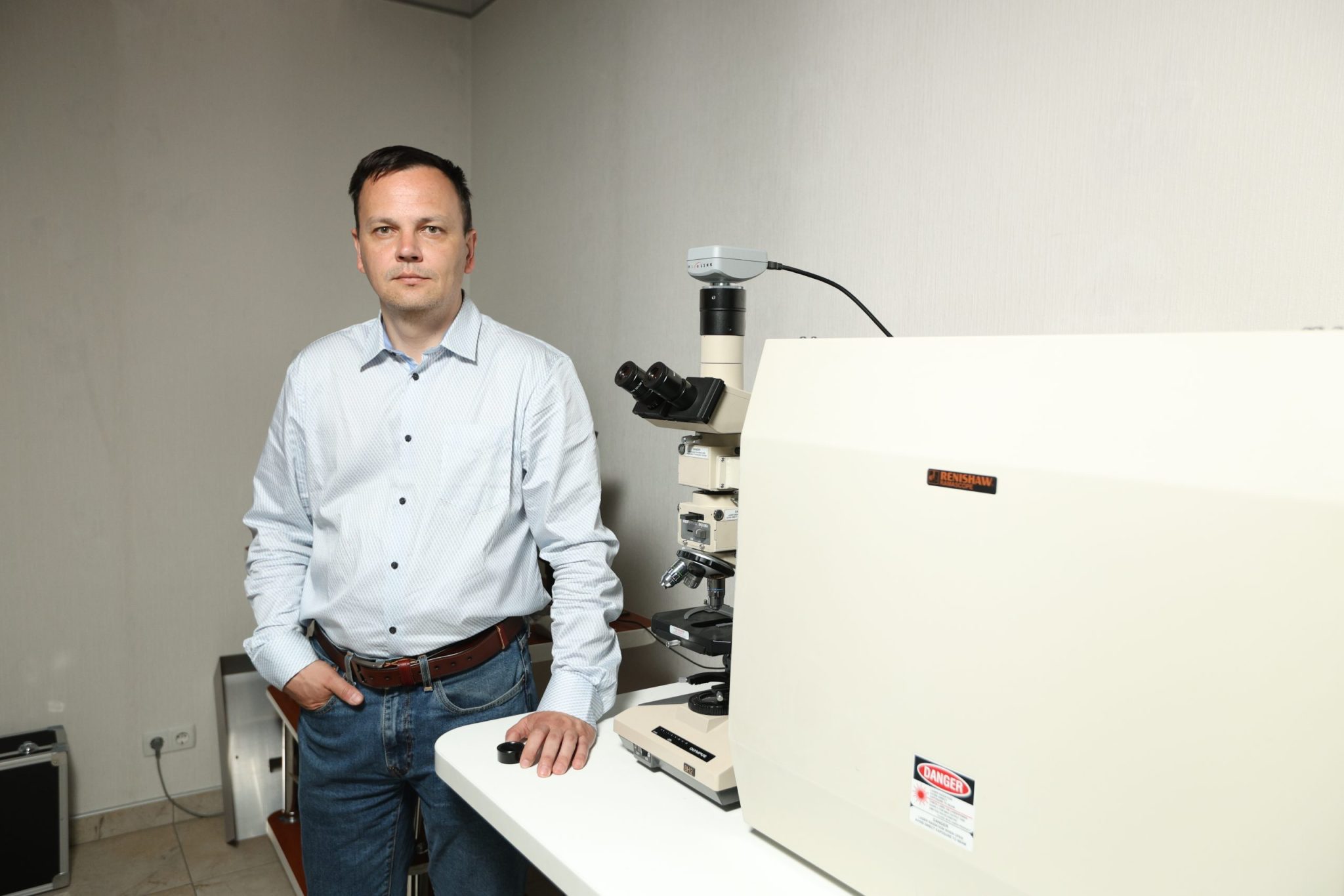
Hit a tiny carbon particle with a powerful laser pulse and it heats to thousands of degrees within nanoseconds and starts to glow. This phenomenon – laser-induced incandescence – is both a measurement method and a research problem in its own right: through it you can see how the particle heats up, evaporates and gives its heat to the surroundings.
The department studies these processes in carbon micro- and nanoparticles – in aqueous suspensions, in porous materials, on transparent heat-sink substrates. The practical outcome ranges from soot and aerosol diagnostics to optical limiters that protect a detector from being blinded by too bright a pulse.
Led by Serhii Zelensky and his group. The standing partner is Shizuoka University in Japan.
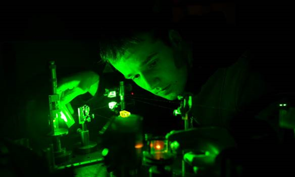
In an ordinary laser, light runs between two mirrors and the resonator sets the wavelength at which lasing begins. In a strongly scattering medium – a powder, a porous material, a dye suspension – there are no mirrors at all, yet lasing still arises: scattering itself takes on the role of the resonator. Light wanders inside long enough to be amplified. This is random lasing.
The department studies how this chaotic lasing interacts with stimulated Raman scattering in the same media: under what conditions the two processes reinforce each other and when they compete. The practical outcome is Raman spectroscopy of substances that give too weak a signal the ordinary way.
Led by Vasyl Yashchuk. Over 90 papers, most of them on laser physics, nonlinear optics and the optics of strongly scattering media.
Optical surface diagnostics
Shine a laser on a rough surface and you will see a grainy pattern – speckle. It looks random, but its statistics are rigidly tied to the relief. So a single shot of the speckle field can measure texture without touching or preparing the sample.
The department showed that the fractal dimension of the speckle pattern correlates with the fractal dimension of the surface itself, and that the method is almost insensitive to defocusing – which means it can be taken from the optical table into a workshop. For ceramic materials of different types the difference in fractal characteristics proved statistically significant: the method distinguishes materials and sees defects. The next step is a portable express-inspection device.
Led by Andrii Yakunov.
The department’s oldest line – the scientific school of “Metal Optics and Surface Spectroellipsometry”, founded by associate professor Mykola Horban, grew out of it.
Ellipsometry measures how reflected light changes its polarisation and from that change reconstructs the material’s optical constants and film thickness – without destroying the sample. For thin metal layers, island gold films and metal-dielectric structures it is practically the only way to learn what is inside.
The practical outcome is plasmonic sensors: a thin gold film on which the surface plasmon resonance shifts when a few molecules land on the surface. For such a sensor to work, the layer’s optical parameters must be known precisely. Polarimetry and colorimetry belong here too.
Led by Oleksii Makarenko and Vadym Prokopets.
Quantum materials and synchrotron research
The direction unfolds in partnership with the Kyiv Academic University: photoemission and X-ray spectroscopy of quantum materials, synchrotron methods – from ARPES to EXAFS. The department belongs to the Ukrainian synchrotron community USynC, whose workshop opens the SPO-2026 symposium, and through these collaborations students gain access to the European XFEL, the SOLARIS synchrotron and the Paul Scherrer Institute. The direction is led by Serhii Kondratenko.
Who we work with
International opportunities for students →
Want to do this with us
A term project, a thesis, doctoral studies – it all starts the same way: you write or come by and say what interests you. You do not need to know the topic in advance, only the direction.
The department’s email is optics.phys@knu.ua, phone +38 067 451 39 02.